
- Nvidia and TSMC have produced the first U.S.-made Blackwell AI wafer at TSMC’s Phoenix, Arizona facility, marking a major milestone for domestic chip production.
- Full chip independence is still years away since advanced packaging remains in Taiwan, though U.S.-based facilities are planned for 2028–2030.
- Nvidia plans to integrate AI, robotics, and automation into future American fabs, aiming to make the U.S. a global hub for AI chip manufacturing.
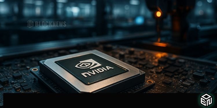
In a milestone moment for the U.S. chip industry, Nvidia and TSMC have officially started producing the first U.S.-made Blackwell AI wafer at TSMC’s high-tech fab in Phoenix, Arizona. The achievement signals a major leap toward strengthening America’s semiconductor independence, especially as global demand for AI and high-performance computing chips skyrockets. Nvidia CEO Jensen Huang joined TSMC executives at the ceremony, calling the moment “a landmark for AI innovation and U.S. manufacturing.”
The Arizona fab is a key part of TSMC’s expansion plan in the U.S., capable of producing chips using advanced 2-, 3-, and 4-nanometer processes. These include Nvidia’s upcoming A16 chips, built specifically for AI data centers, telecom systems, and supercomputing infrastructure. It’s a huge step forward — though not quite full independence yet.
Strengthening America’s Semiconductor Backbone
For Washington, this partnership represents progress under the CHIPS and Science Act, which aims to bring more semiconductor manufacturing back to U.S. soil. The Act provides billions in incentives to reduce America’s dependency on Asia-based production.
“AI is transforming every industry faster than we imagined,” said Huang. “Producing Blackwell in the U.S. is a huge moment not just for Nvidia, but for the entire semiconductor ecosystem.”
TSMC echoed that sentiment, emphasizing that this new facility will play a vital role in supplying chips for next-gen AI systems and supercomputers — all while helping the U.S. reclaim its leadership in high-end chipmaking.
Packaging Still a Bottleneck Overseas
Despite the progress, the U.S. isn’t fully chip-independent yet. While wafer production now happens in Arizona, advanced packaging — known as Chip-on-Wafer-on-Substrate (CoWoS-L) — still takes place in Taiwan. This process fuses multiple chip layers into one powerful AI module, a step that’s critical for Blackwell’s performance.
Industry experts say this packaging gap keeps the U.S. tied to overseas facilities for now. But that’s changing. TSMC recently partnered with Amkor Technology to establish advanced packaging operations in Arizona, with production expected to start between 2028 and 2030. When those lines go live, the U.S. could finally achieve near-complete autonomy in AI chip manufacturing.
The Road Ahead: Robotics, Automation, and AI-Driven Fabs
Looking ahead, Nvidia plans to integrate AI, robotics, and digital twin systems into its future U.S. fabs — pushing automation to a whole new level. TSMC’s Arizona campus is expanding rapidly, with its third fab (Fab 21 P3) set to break ground in 2025. That phase is expected to include CoWoS packaging and serve major clients like Apple, AMD, and Nvidia itself.
Suppliers of high-bandwidth memory (HBM), substrates, and AI packaging equipment are already racing to position themselves for the boom. Analysts predict that once the CoWoS facilities come online, U.S.-based AI chip output could exceed 100,000 units per month by 2026. If all goes according to plan, America could be on track to become one of the world’s key semiconductor powerhouses once again.